- ABOUT LANTECH
- PRODUCTS
Hardened Ethernet Connections
- Introducing Flagship OS5 Switches
- Introducing Layer3 OS3/OS4 Switches
- Introducing Vehicle OS2 PRO Switches
- EN50155 10G Uplinks Managed Ethernet Switches
- EN50155 2.5G Uplinks Managed Ethernet Switches
- EN50155 Giga Uplinks Managed Ethernet Switches
- EN50155 Unmanaged Ethernet Switches
- EN50155 IEC 61375 Ethernet Switches
- EN50155 Rackmount Ethernet Switches
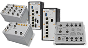
- Tram/Vehicle Switches and Routers (E-Mark / ITxPT)
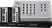
- Industrial Managed Switches
- Industrial 10G Switches
- Industrial 2.5G Switches
- Industrial Rackmount Switches
- Industrial PoE Solutions
- Industrial Unmanaged Switches
- Industrial Converter Series
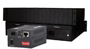
Hardened Routers
Software / Accessories

Naming Rule
- SOLUTIONS
- LEARNING CENTER
- CASE STUDY
- SUPPORT
- NEWS / EVENTS
- CONTACT US
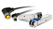
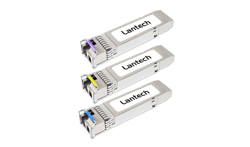
1.25Gbps, WDM1310~1550, Single Fiber Bi-directional SFP, ONU Transceiver
- Distance: 0.5km, 2km, 10km, 20km, 40km, 60km, 80km
- Standard Operating Temperature: -10°C ~ 70°C
- Wide Operating Temperature: -40°C ~ 85°C
OVERVIEW
Lantech 1.25Gbps Bi-directional (BiDi) Small Form Factor Pluggable (SFP) transceiver module series is specifically designed for the high performance integrated duplex data link over a single optical fiber. These transceiver modules are compliant with the SFP Multisource Agreement (MSA). With the hot pluggability, these modules offer an easy way to be installed into SFP MSA compliant ports at any time without the interruption of the host equipments operating online.
Lantech 1.25Gbps BiDi SFP transceiver module series using a long wavelength FP/DFB laser diode and enable data transmission up to 80km on a single-mode (9/125μm) optical fiber. (0.5km on a multi-mode optical fiber)
FEATURES
- 1.25G bi-directional single-fiber link
- Single LC receptacle
- 1310~1550nm FP/DFB transmitter
- 1310~1550nm PIN receiver
- 0.5km to 80km point-to-point transmission
- Compliant with IEEE802.3ah Standard
- Compliant with SFF8472 diagnostic monitoring interface
- Compliant with SFP MSA
- Hot Pluggable
- RoHS Compliant
SPECIFICATIONS
Absolute Maximum Ratings
Parameter |
Symbol |
Min. |
Max. |
Unit |
Note |
Storage Temperature |
Ts |
-40 |
+85 |
°C |
|
Supply Voltage |
VccT, VccR |
-0.5 |
4.0 |
V |
|
Storage Relative Humidity |
RH |
5 |
95 |
% |
|
Recommended Operating Conditions (10km, 20km, 40km, 60km, 80km)
Parameter |
Symbol |
Min. |
Typ. |
Max. |
Unit |
Note |
||
Case Operating Temperature |
Tc |
-10 / -40 |
|
70 / 85 |
°C |
1 |
||
Supply Voltage |
Vcc |
3.1 |
3.3 |
3.5 |
V |
|
||
Supply Current |
Icc |
|
180 |
280 |
mA |
|
||
Notes: 1. Standard Operating Temperature / Wide Operating Temperature (-E model) |
||||||||
Recommended Operating Conditions (0.5km, 2km)
Parameter |
Symbol |
Min. |
Typ. |
Max. |
Unit |
Note |
||
Case Operating Temperature |
Tc |
-10 / -40 |
|
70 / 85 |
°C |
1 |
||
Supply Voltage |
Vcc |
3.15 |
3.3 |
3.45 |
V |
|
||
Supply Current |
Icc |
|
180 |
280 |
mA |
|
||
Notes: 1. Standard Operating Temperature / Wide Operating Temperature (-E model) |
||||||||
Transmitter Electro-Optical Characteristics
Parameter |
Symbol |
Min. |
Typ. |
Max. |
Unit |
Note |
||
Optical Launch Power |
0.5km |
WDM1310 |
Po |
-10 |
|
0 |
dBm |
1 |
WDM1550 |
-10 |
0 |
||||||
2km |
WDM1310 |
-11 |
-3 |
|||||
WDM1550 |
-11 |
-3 |
||||||
10km |
WDM1310 |
-9 |
-3 |
|||||
WDM1550 |
-9 |
-3 |
||||||
20km |
WDM1310 |
-8 |
-2 |
|||||
WDM1550 |
-8 |
-2 |
||||||
40km |
WDM1310 |
-3 |
+2 |
|||||
WDM1550 |
-5 |
0 |
||||||
60km |
WDM1310 |
0 |
+5 |
|||||
WDM1550 |
-3 |
+4 |
||||||
80km |
WDM1490 |
-2 |
+4 |
|||||
WDM1550 |
-2 |
+4 |
||||||
Optical Extinction Ratio |
ER |
9 |
|
|
dB |
|
||
Center Wavelength |
0.5km |
WDM1310 |
λC |
1270 |
1310 |
1355 |
nm |
|
WDM1550 |
1510 |
1550 |
1570 |
|||||
2km |
WDM1310 |
1270 |
1310 |
1355 |
||||
WDM1550 |
1510 |
1550 |
1570 |
|||||
10km |
WDM1310 |
1270 |
1310 |
1355 |
||||
WDM1550 |
1510 |
1550 |
1570 |
|||||
20km |
WDM1310 |
1270 |
1310 |
1355 |
||||
WDM1550 |
1510 |
1550 |
1570 |
|||||
40km |
WDM1310 |
1270 |
1310 |
1355 |
||||
WDM1550 |
1510 |
1550 |
1570 |
|||||
60km |
WDM1310 |
1270 |
1310 |
1355 |
||||
WDM1550 |
1510 |
1550 |
1570 |
|||||
80km |
WDM1490 |
1480 |
1490 |
1500 |
||||
WDM1550 |
1530 |
1550 |
1570 |
|||||
Spectral Width |
0.5km |
WDM1310 |
Δλ |
|
|
4 |
nm |
RMS |
WDM1550 |
4 |
|||||||
2km |
WDM1310 |
2.5 |
||||||
WDM1550 |
2.5 |
|||||||
10km |
WDM1310 |
2.5 |
||||||
WDM1550 |
1 |
-20dB |
||||||
20km |
WDM1310 |
2.5 |
RMS |
|||||
WDM1550 |
1 |
-20dB |
||||||
40km |
WDM1310 |
1 |
||||||
WDM1550 |
1 |
|||||||
60km |
WDM1310 |
1 |
||||||
WDM1550 |
1 |
|||||||
80km |
WDM1490 |
1 |
||||||
WDM1550 |
1 |
|||||||
Optical Rise / Fall Timet |
tr / tf |
|
|
260 |
ps |
|
||
Relative Intensity Noise |
RIN |
|
|
-120 |
dB/Hz |
|
||
Total Contributed Jitter |
TJ |
|
|
227 |
ps |
|
||
Optical Eye Mask |
|
IEEE802.3z |
|
|||||
Differential Data Input Noise |
VDIFF |
400 |
|
2000 |
mV |
|
||
Transmit Disable Voltage |
Vdis |
2.0 |
|
Vcc |
V |
|
||
Transmit Enable Voltage |
Ven |
GND |
|
GND+0.8 |
V |
|
||
Notes: 1. The optical power is launched into a 9/125μm single-mode fiber. (2km, 10km, 20km, 40km, 60km, 80km) |
||||||||
Receiver Electro-Optical Characteristics
Parameter |
Symbol |
Min. |
Typ. |
Max. |
Unit |
Note |
||
Maximum Input Power |
PINMAX |
-3 |
|
|
|
1 |
||
Receiver Sensitivity |
0.5km |
WDM1310 |
PINMIN |
|
|
-20 |
dBm |
1 |
WDM1550 |
||||||||
2km |
WDM1310 |
|||||||
WDM1550 |
||||||||
10km |
WDM1310 |
|||||||
WDM1550 |
||||||||
20km |
WDM1310 |
-23 |
||||||
WDM1550 |
||||||||
40km |
WDM1310 |
-23 |
||||||
WDM1550 |
||||||||
60km |
WDM1310 |
-24 |
||||||
WDM1550 |
-25 |
|||||||
80km |
WDM1490 |
-25 |
||||||
WDM1550 |
||||||||
Operating Center Wavelength |
0.5km |
WDM1310 |
λc |
1470 |
|
1600 |
nm |
|
WDM1550 |
1250 |
1380 |
||||||
2km |
WDM1310 |
1470 |
|
1600 |
||||
WDM1550 |
1250 |
1380 |
||||||
10km |
WDM1310 |
1470 |
|
1600 |
||||
WDM1550 |
1250 |
1380 |
||||||
20km |
WDM1310 |
1470 |
|
1600 |
||||
WDM1550 |
1250 |
1380 |
||||||
40km |
WDM1310 |
1470 |
|
1600 |
||||
WDM1550 |
1250 |
1380 |
||||||
60km |
WDM1310 |
1470 |
|
1600 |
||||
WDM1550 |
1250 |
1380 |
||||||
80km |
WDM1490 |
1530 |
1550 |
1570 |
||||
WDM1550 |
1470 |
1490 |
1510 |
|||||
Optical Return Loss |
ORL |
12 |
|
|
dB |
|
||
LOS De-Assert |
0.5km |
WDM1310 |
LOSD |
|
|
-21 |
dBm |
|
WDM1550 |
||||||||
2km |
WDM1310 |
-20 |
||||||
WDM1550 |
||||||||
10km |
WDM1310 |
-20 |
||||||
WDM1550 |
||||||||
20km |
WDM1310 |
-23 |
||||||
WDM1550 |
||||||||
40km |
WDM1310 |
-23 |
||||||
WDM1550 |
||||||||
60km |
WDM1310 |
-24 |
||||||
WDM1550 |
-25 |
|||||||
80km |
WDM1490 |
-25 |
||||||
WDM1550 |
||||||||
LOS Assert |
LOSA |
-35 |
|
|
dBm |
|
||
LOS Hysteresis |
LOSHY |
0.5 |
|
|
dB |
|
||
Differential Data Output Voltage |
Vout, pp |
500 |
|
1200 |
mV |
|
||
Data Output Rise/Fall Time (20%~80%) |
Tr/Tf |
|
|
0.35 |
ns |
|
||
Receiver LOS Signal Output Voltage-Low |
LOSVL |
GND |
|
GND+0.5 |
V |
|
||
Receiver LOS Signal Output Voltage-High |
LOSVH |
2.4 |
|
Vcc |
V |
|
||
| Notes: 1. Measured with a PRBS 27 -1 test pattern @ 1.25Gbps BER < 10-12 | ||||||||
Pin Assignment
|
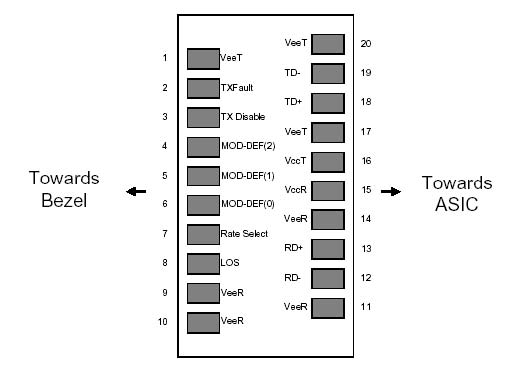
Pin Description
Pin |
Name |
Function / Description |
1 |
VeeT |
Transmitter Ground |
2 |
TX_Fault |
Transmitter Fault Indication (1) |
3 |
TX_Disable |
Transmission Disable – Module disables on high or open (2) |
4 |
MOD-DEF(2) |
Module Definition 2 – SDA: Serial Data Signal |
5 |
MOD-DEF(1) |
Module Definition 1 – SCL: Serial Clock Signal |
6 |
MOD-DEF(0) |
Module Definition 0 – LVTTL Low (3) |
7 |
Rate Select |
Not Connected – Open Circuit |
8 |
LOS |
Receiver Loss of Signal (4) |
9 |
VeeR |
Receiver Ground |
10 |
VeeR |
Receiver Ground |
11 |
VeeR |
Receiver Ground |
12 |
RD- |
Inverse Received Data out, Differential LVPECL, AC coupled |
13 |
RD+ |
Received Data out, Differential LVPECL, AC coupled |
14 |
VeeR |
Receiver Ground |
15 |
VccR |
Receiver Power |
16 |
VccT |
Transmitter Power |
17 |
VeeT |
Transmitter Ground |
18 |
TD+ |
Transmitter Data In, Differential LVPECL, AC coupled |
19 |
TD- |
Inverse Transmitter Data In, Differential LVPECL, AC coupled |
20 |
Veet |
Transmitter Ground |
Note1: TX Fault is open collector/drain output which should be pulled up externally with a 4.7K~ 10KΩ resistor on the host board to supply <VccT+0.3V or VccR+0.3V. When high, this output indicates a laser fault of some kind. Low indicates normal operation. In the low state, the output will be pulled to <0.8V. |
||
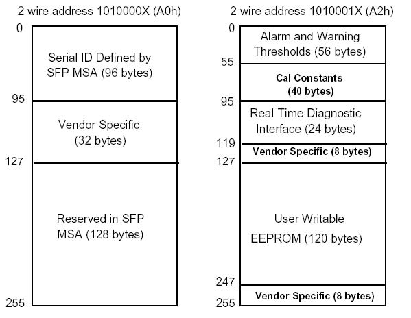
Digital Diagnostic Functions
As defined by the SFP MSA (SFF-8472) Lantech’s SFP transceivers provide digital diagnostic functions via a 2-wire serial interface, which allows real-time access to the following operating parameters:
- Transceiver temperature
- Laser bias current
- Transmitted optical power
- Received optical power
- Transceiver supply voltage
It also provides a sophisticated system of alarm and warning flags, which may be used to alert end-users when particular operating parameters are outside of a factory-set normal range.
The operating and diagnostics information is monitored and reported by a Digital Diagnostics Controller (DDC) inside the transceiver, which is accessed through the 2-wire serial interface. When the serial protocol is activated, the serial clock signal (SCL pin) is generated by the host. The positive edge clocks data into the SFP transceiver into those segments of its memory map that are not write-protected. The negative edge clocks data from the SFP transceiver. The serial data signal (SDA pin) is bi-directional for serial data transfer. The host uses SDA in conjunction with SCL to mark the start and end of serial protocol activation. The memories are organized as a series of 8-bit data words that can be addressed individually or sequentially.
For more detailed information including memory map definitions, please see the SFP MSA (SFF-8472) Specification.
Digital Diagnostic Memory Map
|
Digital Diagnostic Monitoring Characteristics
Parameter |
Accuracy |
Unit |
Note |
Temperature |
±3 |
°C |
|
Supply Voltage |
±0.1 |
V |
|
TX Bias Current |
±5 |
mA |
|
TX Output Power |
±3 |
dB |
|
RX Received Optical Power |
±3 |
dB |
|
DIMENSION
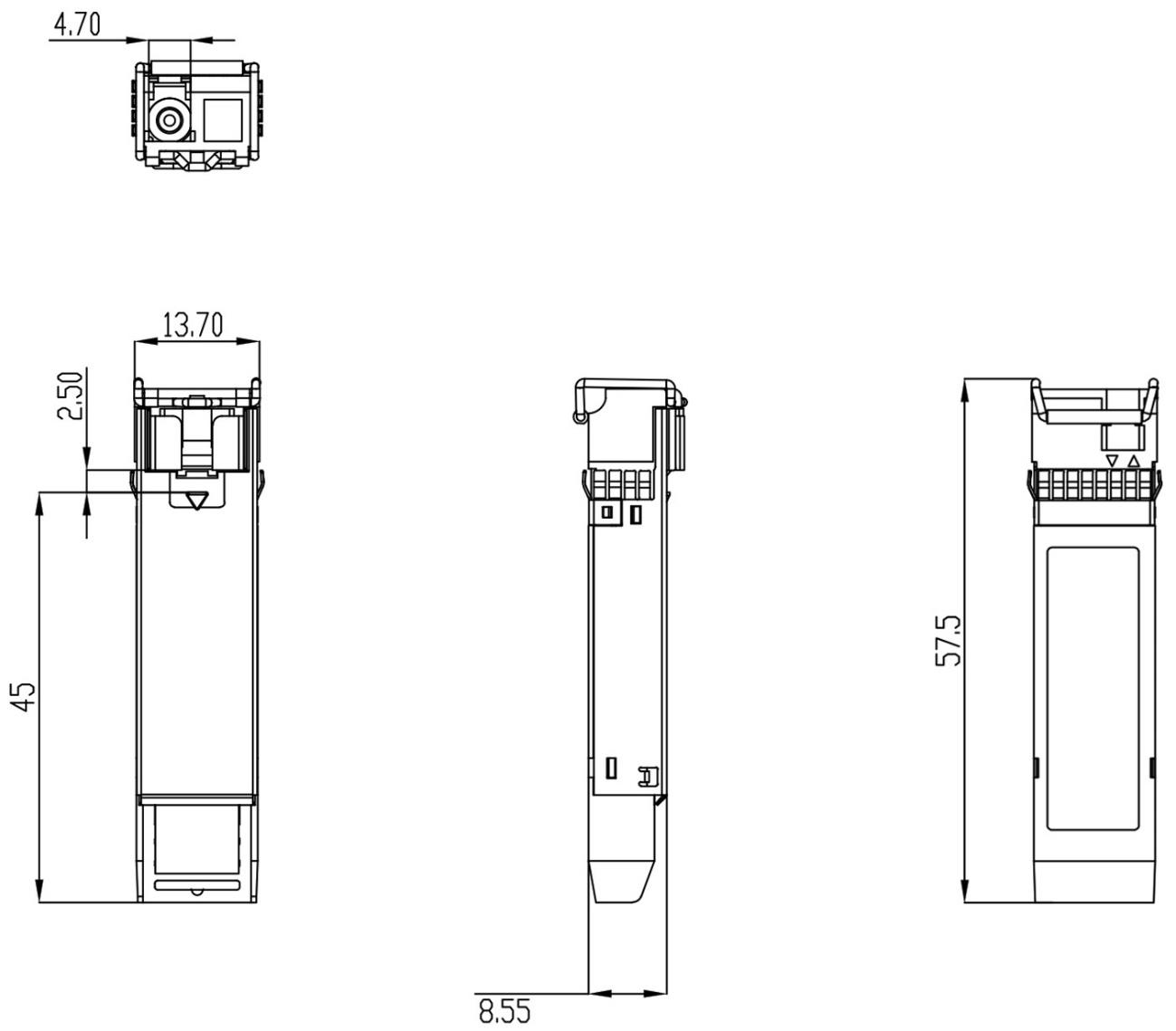 *All dimensions are ±0.2mm unless otherwise specified
ORDERING INFORMATION
Part Number |
TX |
LD |
RX |
IO |
LOS |
Link |
Mode |
Temp. |
8330-197D-V1 |
1310nm |
FP |
1550nm |
AC/AC |
TTL |
0.5km |
Multi-mode |
-10~70°C |
8330-195D-V1 |
FP |
2km |
Single-mode |
|||||
8330-188D-V1 |
FP |
10km |
Single-mode |
|||||
8330-186D-V1 |
FP |
20km |
Single-mode |
|||||
8330-180D-V1 |
DFB |
40km |
Single-mode |
|||||
8330-181D-V1 |
DFB |
60km |
Single-mode |
|||||
8330-184D-V1 |
1490nm |
DFB |
80km |
Single-mode |
Part Number |
TX |
LD |
RX |
IO |
LOS |
Link |
Mode |
Temp. |
8330-197DE-V1 |
1310nm |
FP |
1550nm |
AC/AC |
TTL |
0.5km |
Multi-mode |
-40~85°C |
8330-195DE-V1 |
FP |
2km |
Single-mode |
|||||
8330-188DE-V1 |
FP |
10km |
Single-mode |
|||||
8330-186DE-V1 |
FP |
20km |
Single-mode |
|||||
8330-180DE-V1 |
DFB |
40km |
Single-mode |
|||||
8330-181DE-V1 |
DFB |
60km |
Single-mode |
|||||
8330-184DE-V1 |
1490nm |
DFB |
80km |
Single-mode |
Part Number |
TX |
LD |
RX |
IO |
LOS |
Link |
Mode |
Temp. |
8330-198D-V1 |
1550nm |
FP |
1310nm |
AC/AC |
TTL |
0.5km |
Multi-mode |
-10~70°C |
8330-196D-V1 |
2km |
Single-mode |
||||||
8330-189D-V1 |
DFB |
10km |
Single-mode |
|||||
8330-187D-V1 |
20km |
Single-mode |
||||||
8330-182D-V1 |
40km |
Single-mode |
||||||
8330-183D-V1 |
60km |
Single-mode |
||||||
8330-185D-V1 |
1490nm |
80km |
Single-mode |
Part Number |
TX |
LD |
RX |
IO |
LOS |
Link |
Mode |
Temp. |
8330-198DE-V1 |
1550nm |
FP |
1310nm |
AC/AC |
TTL |
0.5km |
Multi-mode |
-40~85°C |
8330-196DE-V1 |
2km |
Single-mode |
||||||
8330-189DE-V1 |
DFB |
10km |
Single-mode |
|||||
8330-187DE-V1 |
20km |
Single-mode |
||||||
8330-182DE-V1 |
40km |
Single-mode |
||||||
8330-183DE-V1 |
60km |
Single-mode |
||||||
8330-185DE-V1 |
1490nm |
80km |
Single-mode |