- ABOUT LANTECH
- PRODUCTS
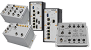
Hardened Ethernet Connections
- Introducing Flagship OS5 Switches
- Introducing Layer3 OS3/OS4 Switches
- Introducing Vehicle OS2 PRO Switches
- EN50155 10G Uplinks Managed Ethernet Switches
- EN50155 2.5G Uplinks Managed Ethernet Switches
- EN50155 Giga Uplinks Managed Ethernet Switches
- EN50155 Unmanaged Ethernet Switches
- EN50155 IEC 61375 Ethernet Switches
- EN50155 Rackmount Ethernet Switches
- Tram/Vehicle Switches and Routers (E-Mark / ITxPT)
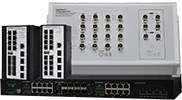
- Industrial Managed Switches
- Industrial 10G Switches
- Industrial 2.5G Switches
- Industrial Rackmount Switches
- Industrial PoE Solutions
- Industrial Unmanaged Switches
- Industrial Converter Series
Hardened Routers
Software / Accessories

Naming Rule
- SOLUTIONS
- LEARNING CENTER
- CASE STUDY
- SUPPORT
- NEWS / EVENTS
- CONTACT US
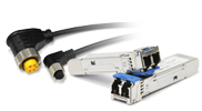
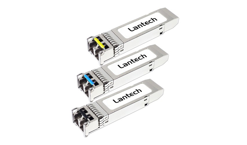
1310nm DFB, Duplex LC, 2.5GBase-X SFP Transceiver
- Distance: 15km
- Standard Operating Temperature: -10°C ~ 70°C
- Wide Operating Temperature: -40°C ~ 85°C
OVERVIEW
Lantech 2.5GBase-X Small Form Factor Pluggable SFP transceivers are compliant with the current SFP Multi-Source Agreement (MSA) Specification. The high performance 1310nm DFB transmitter and high sensitive PIN receiver provide superior performance for SONET/SDH applications up to 15km optical links with single mode fiber.
FEATURES
- Compliant with SONET OC-48 IR1 and SDH STM-16 S16.1 Standard
- Compliant with 2500Base-X
- Compliant with SFP MSA
- Compliant with SFP8472 diagnostic monitoring interface
- Hot Pluggable
- 1310nm DFB laser transmitter
- Duplex LC connector
- 2-wire interface for management and diagnostic monitor
- Single +3.3V power supply
- Transmission distance of 15km over single mode fiber
- RoHS Compliant
SPECIFICATIONS
Absolute Maximum Ratings
Parameter |
Symbol |
Min. |
Max. |
Unit |
Note |
Storage Temperature |
TST |
-40 |
+85 |
°C |
|
Supply Voltage |
Vcc |
-0.5 |
4.0 |
V |
|
Storage Relative Humidity |
RH |
5 |
95 |
% |
|
Recommended Operating Conditions
Parameter |
Symbol |
Min. |
Typ. |
Max. |
Unit |
Note |
Case Operating Temperature |
TOP |
-10 |
|
70 |
°C |
|
Case Operating Temperature |
TOP |
-40 |
|
85 |
°C |
|
Supply Voltage |
Vcc |
+3.15 |
+3.3 |
+3.45 |
V |
|
Supply Current |
ICC |
|
200 |
260 |
mA |
|
Transmitter Electro-Optical Characteristics
Parameter |
Symbol |
Min. |
Typ. |
Max. |
Unit |
Note |
||
Optical launch Power |
PO |
-5 |
|
0 |
dBm |
1 |
||
Center Wavelength |
λC |
1280 |
1310 |
1340 |
nm |
|
||
Spectral Width (RMS) |
Δλ |
|
|
1 |
nm |
|
||
Side Mode Suppression Ratio |
SMSR |
|
|
30 |
dB |
|
||
Optical Extinction Ratio |
ER |
8.2 |
|
|
dB |
|
||
Rise/Fall Time (10%~90%) |
Tr/Tf |
|
|
0.16 |
ns |
|
||
Optical Eye Mask |
|
ITU-T G.957 STM-16 |
|
|||||
Differential Data Input Voltage |
VDIFF |
300 |
|
1600 |
mV |
|
||
Transmit Disable Voltage |
VDIS |
2.0 |
|
Vcc |
V |
|
||
Transmit Enable Voltage |
VEN |
GND |
|
GND+0.8 |
V |
|
||
Notes: 1. The optical power is launched into a 9/125μm single-mode fiber. |
||||||||
Receiver Electro-Optical Characteristics
Parameter |
Symbol |
Min. |
Typ. |
Max. |
Unit |
Note |
||
Receiver Sensitivity |
PINMIN |
|
|
-18 |
dBm |
1 |
||
Maximum Input Power |
PINMAX |
-3 |
|
|
dBm |
1 |
||
Operating Center Wavelength |
λC |
1100 |
|
1610 |
nm |
|
||
LOS De-Assert |
LOSD |
|
|
-18 |
dBm |
|
||
LOS Assert |
LOSA |
-30 |
|
|
dBm |
|
||
LOS Hysteresis |
LOSVHY |
0.5 |
|
|
dB |
|
||
Differential Data Output Voltage |
Vout, pp |
300 |
|
1000 |
mV |
|
||
Data Output Rise/Fall Time (10%~90%) |
Tr/Tf |
|
|
0.18 |
ns |
|
||
Receiver LOS Signal Output Voltage-Low |
LOSVL |
GND |
|
GND+0.5 |
V |
|
||
Receiver LOS Signal Output Voltage-High |
LOSVH |
2.4 |
|
Vcc |
V |
|
||
Notes: 1. Measured with a PRBS 231-1 test pattern @ 2488Mbps BER < 10-10 |
||||||||
Pin Assignment
|
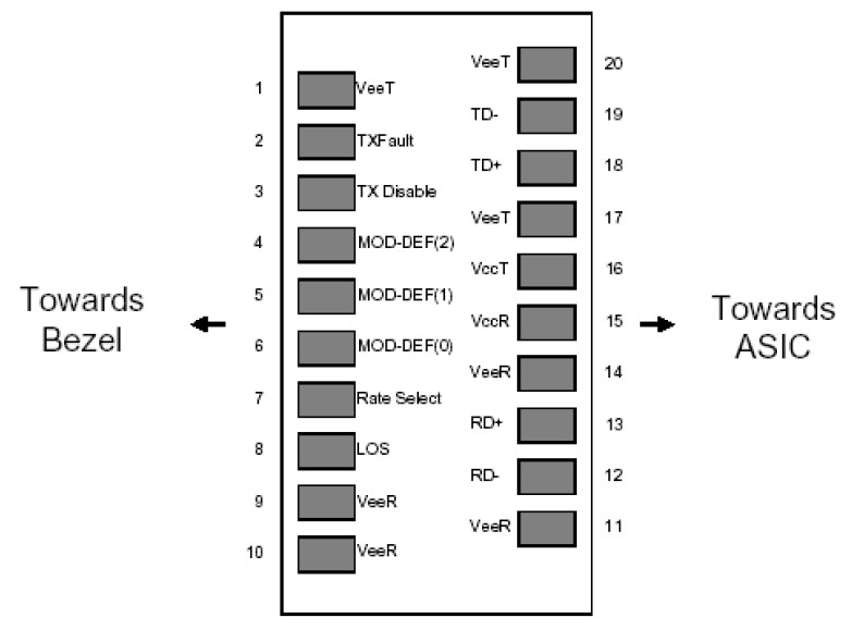
Pin Description
Pin |
Name |
Function / Description |
1 |
VeeT |
Transmitter Ground |
2 |
TX_Fault |
Transmitter Fault Indication (1) |
3 |
TX_Disable |
Transmission Disable – Module disables on high or open (2) |
4 |
MOD-DEF(2) |
Module Definition 2 – SDA: Serial Data Signal |
5 |
MOD-DEF(1) |
Module Definition 1 – SCL: Serial Clock Signal |
6 |
MOD-DEF(0) |
Module Definition 0 – LVTTL Low (3) |
7 |
Rate Select |
Not Connected – Open Circuit |
8 |
LOS |
Receiver Loss of Signal (4) |
9 |
VeeR |
Receiver Ground |
10 |
VeeR |
Receiver Ground |
11 |
VeeR |
Receiver Ground |
12 |
RD- |
Inverse Received Data out, Differential LVPECL, AC coupled |
13 |
RD+ |
Received Data out, Differential LVPECL, AC coupled |
14 |
VeeR |
Receiver Ground |
15 |
VccR |
Receiver Power |
16 |
VccT |
Transmitter Power |
17 |
VeeT |
Transmitter Ground |
18 |
TD+ |
Transmitter Data In, Differential LVPECL, AC coupled |
19 |
TD- |
Inverse Transmitter Data In, Differential LVPECL, AC coupled |
20 |
VeeT |
Transmitter Ground |
Note1: TX Fault is open collector/drain output which should be pulled up externally with a 4.7K~ 10KΩ resistor on the host board to supply <VccT+0.3V or VccR+0.3V. When high, this output indicates a laser fault of some kind. Low indicates normal operation. In the low state, the output will be pulled to <0.8V. |
||
DIMENSION
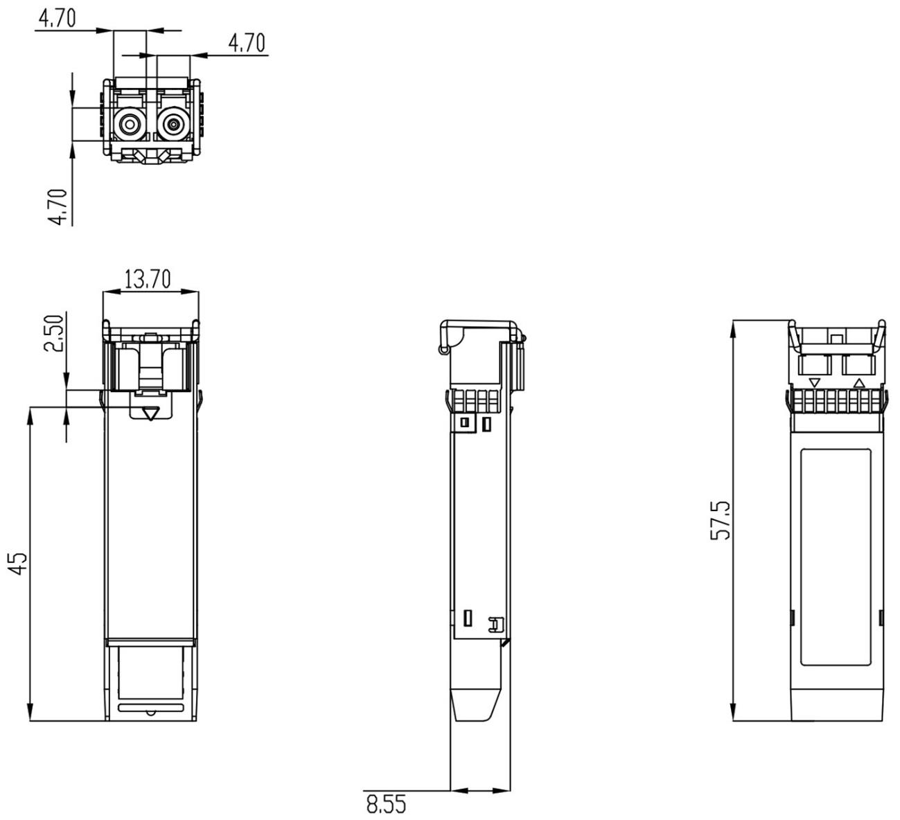 *All dimensions are ±0.2mm unless otherwise specified
ORDERING INFORMATION
Part Number |
TX |
Link |
Mode |
Temp. |
||||
8330-265D-V1 |
1310nm |
15km |
Single-mode |
-10~70°C |
||||
8330-265DE-V1 |
1310nm |
15km |
Single-mode |
-40~85°C |
||||
| All SFP P/N# ended with D are with DDM function | ||||||||