- ABOUT LANTECH
- PRODUCTS
Hardened Ethernet Connections
- Introducing Flagship OS5 Switches
- Introducing Layer3 OS3/OS4 Switches
- Introducing Vehicle OS2 PRO Switches
- EN50155 10G Uplinks Managed Ethernet Switches
- EN50155 2.5G Uplinks Managed Ethernet Switches
- EN50155 Giga Uplinks Managed Ethernet Switches
- EN50155 Unmanaged Ethernet Switches
- EN50155 IEC 61375 Ethernet Switches
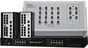
- EN50155 Rackmount Ethernet Switches
- Tram/Vehicle Switches and Routers (E-Mark / ITxPT)
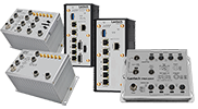
- Industrial Managed Switches
- Industrial 10G Switches
- Industrial 2.5G Switches
- Industrial Rackmount Switches
- Industrial PoE Solutions
- Industrial Unmanaged Switches
- Industrial Converter Series
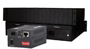
Hardened Routers
Software / Accessories

Naming Rule
- SOLUTIONS
- LEARNING CENTER
- CASE STUDY
- SUPPORT
- NEWS / EVENTS
- CONTACT US
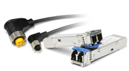
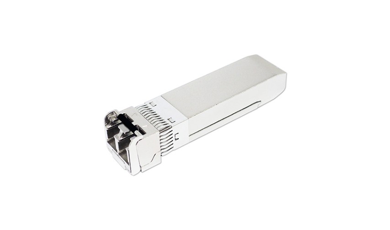
10G SFP+ LR (ER-1310/ER-1550) Transceiver
- Hot Pluggable, Duplex LC, 1310nm DFB/1550nm EML, Single Mode, DDM
- Distance: 40KM
- Standard Operating Temperature: 0°C ~ 70°C
- Wide Operating Temperature: -40°C ~ 85°C
OVERVIEW
10GBase-LR/LW Small Form Factor Pluggable SFP+ transceivers are compliant with the current SFP+ Multi-Source Agreement (MSA) Specification. The high performance uncooled 1310nm DFB/1550nm EML transmitter and high sensitivity PIN receiver provide superior performance for 10GBASE-LR/LW applications up to SMF 40km optical links.
FEATURES
- Compliant with IEEE802.3ae 10GBASE-LR/LW
- Compliant with CPRI Option 7, 8
- Compliant with SFF-8431 SFP+ MSA
- Support 8.5Gb/s to 11.32Gb/s Multi-Rate
- Hot Pluggable
- 1310nm DFB/1550nm EML laser transmitter
- Duplex LC connector
- 2-wire interface for management and diagnostic monitor compliant with SFF-8472
- Single +3.3V power supply
- Link distance 40km over SM fiber
- RoHS Compliant
SPECIFICATIONS
Absolute Maximum Ratings
Parameter |
Symbol |
Min. |
Max. |
Unit |
Note |
Storage Temperature |
Ts |
-40 |
+85 |
°C |
|
Supply Voltage |
Vcc |
-0.5 |
+4.0 |
V |
|
Storage Relative Humidity |
RH |
5 |
95 |
% |
|
Operational Humidity |
RH |
0 |
85 |
% |
|
Recommended Operating Conditions
Parameter |
Symbol |
Min. |
Typ. |
Max. |
Unit |
Note |
Case Operating Temperature |
Top |
0 |
|
+70 |
°C |
|
Case Operating Temperature (-E model) |
Top |
-40 |
|
+85 |
°C |
|
Supply Voltage |
Vcc |
+3.13 |
+3.3 |
+3.47 |
V |
|
Supply Current |
Icc |
|
|
350 |
mA |
|
Supply Current (-E model) |
Icc |
|
|
380 |
mA |
|
Transmitter Electro-Optical Characteristics
VCC= 3.13V to 3.47V, TOP = 0 °C to 70 °C (standard model); TOP = -40 °C to 85 °C (-E model)
Parameters |
Symbol |
Min. |
Typ. |
Max. |
Unit |
Note |
||
Operating Date Rate |
DR |
8.5 |
10.3125 |
11.32 |
Gb/s |
|
||
Optical Launch Power |
Po |
0 |
|
+4 |
dBm |
1 |
||
Optical Center Wavelength |
λc |
1260 |
1310 |
1355 |
nm |
|
||
Spectral Width (-20dB) |
△λ |
|
|
1 |
nm |
|
||
Side Mode Suppression Ratio |
SMSR |
30 |
|
|
dB |
|
||
Optical Extinction Ratio |
ER |
3.5 |
|
|
dB |
|
||
Optical Eye Mask |
|
IEEE802.3ae |
|
|||||
Relative Intensity Noise |
RIN |
|
|
-128 |
dB/Hz |
|
||
Differential Data Input Swing |
VIN |
180 |
|
850 |
mV |
|
||
TX Disable Input Voltage-Low (TX ON) |
TDISVL |
GND |
|
0.8 |
V |
|
||
TX Disable Input Voltage-High (TX OFF) |
TDISVH |
2.0 |
|
Vcc |
V |
|
||
TX Fault Output Voltage-Low (TX Normal) |
TFLTVL |
GND |
|
0.8 |
V |
|
||
TX Fault Output Voltage-High (TX Fault) |
TFLTVH |
2.0 |
|
Vcc |
V |
|
||
Notes: 1. The optical power is launched into a 9/125μm single-mode fiber |
||||||||
Receiver Electro-Optical Characteristics
VCC= 3.13V to 3.47V, TOP = 0 °C to 70 °C (standard model); TOP = -40 °C to 85 °C (-E model)
Parameters |
Symbol |
Min. |
Typ. |
Max. |
Unit |
Note |
||
Operating Date Rate |
DR |
8.5 |
10.3125 |
11.32 |
Gb/s |
|
||
Receiver Sensitivity |
PIN_min |
|
|
-16 |
dBm |
1 |
||
Maximum Input Power |
PIN_max |
+0.5 |
|
|
dBm |
1 |
||
Optical Center Wavelength |
λC |
1260 |
|
1620 |
nm |
|
||
LOS De-Assert |
LOSD |
|
|
-17 |
dBm |
|
||
LOS Assert |
LOSA |
-30 |
|
|
dBm |
|
||
LOS Hysteresis |
LOSHY |
0.5 |
|
|
dB |
|
||
Differential data output voltage |
Vout |
300 |
|
900 |
mV |
|
||
Receiver LOS Signal Output Voltage-Low |
LOSVL |
GND |
|
0.8 |
V |
|
||
Receiver LOS Signal Output Voltage-High |
LOSVH |
2.0 |
|
Vcc |
V |
|
||
Note1: Measured with a PRBS 231-1 test pattern @10.3125Gbps BER<10-12 |
||||||||
Pin Assignment
|
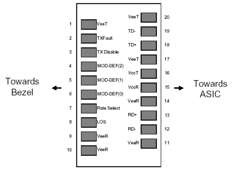
Pin Description
Pin |
Name |
Function / Description |
1 |
VeeT |
Transmitter Ground |
2 |
TX_Fault |
Transmitter Fault Indication (1) |
3 |
TX_Disable |
Transmitter Disable – Turns off transmitter laser output (2) |
4 |
SDA |
2-wire Serial Interface Data Line (SDA: Serial Data Signal) (3) |
5 |
SCL |
2-wire Serial Interface Clock (SCL: Serial Clock Signal) (3) |
6 |
Mod_ABS |
Module Absent, connected to VeeT or VeeR in the module (3) |
7 |
RS0 |
Rate Select 0, optional (5) |
8 |
Rx_LOS |
Receiver Loss of Signal Indication (4) |
9 |
RS1 |
Rate Select 1, optional (5) |
10 |
VeeR |
Receiver Ground |
11 |
VeeR |
Receiver Ground |
12 |
RD- |
Receiver Inverted Data output, AC coupled |
13 |
RD+ |
Receiver Non-Inverted Data output, AC coupled |
14 |
VeeR |
Receiver Ground |
15 |
VccR |
Receiver 3.3V Power Supply |
16 |
VccT |
Transmitter 3.3V Power Supply |
17 |
VeeT |
Transmitter Ground |
18 |
TD+ |
Transmitter Non-Inverted Data Input, AC coupled |
19 |
TD- |
Transmitter Inverted Data Input, AC coupled |
20 |
VeeT |
Transmitter Ground |
Note1: TX Fault is open collector/drain output which should be pulled up externally with a 4.7K~10KΩ resistor on the host board to supply <VccT+0.3V or VccR+0.3V. When high, this output indicates a laser fault of some kind. Low indicates normal operation. In the low state, the output will be pulled to <0.8V. |
||
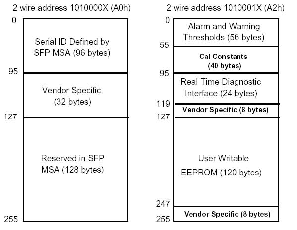
Digital Diagnostic Functions
As defined by the SFP MSA (SFF-8472) Lantech’s SFP transceivers provide digital diagnostic functions via a 2-wire serial interface, which allows real-time access to the following operating parameters:
- Transceiver temperature
- Laser bias current
- Transmitted optical power
- Received optical power
- Transceiver supply voltage
It also provides a sophisticated system of alarm and warning flags, which may be used to alert end-users when particular operating parameters are outside of a factory-set normal range.
The operating and diagnostics information is monitored and reported by a Digital Diagnostics Controller (DDC) inside the transceiver, which is accessed through the 2-wire serial interface. When the serial protocol is activated, the serial clock signal (SCL pin) is generated by the host. The positive edge clocks data into the SFP+ transceiver into those segments of its memory map that are not write-protected. The negative edge clocks data from the SFP+ transceiver. The serial data signal (SDA pin) is bi-directional for serial data transfer. The host uses SDA in conjunction with SCL to mark the start and end of serial protocol activation. The memories are organized as a series of 8-bit data words that can be addressed individually or sequentially.
For more detailed information including memory map definitions, please see the SFP MSA (SFF-8472) Specification.
Digital Diagnostic Memory Map
Digital Diagnostic Monitoring Characteristics Map
Parameter |
Accuracy |
Unit |
Note |
Temperature |
±3 |
℃ |
Internal Calibration |
Supply Voltage |
±0.1 |
V |
Internal Calibration |
TX Bias Current |
±5 |
mA |
Internal Calibration |
TX Output Power |
±3 |
dB |
Internal Calibration |
RX Received Optical Power |
±3 |
dB |
Internal Calibration |
DIMENSION
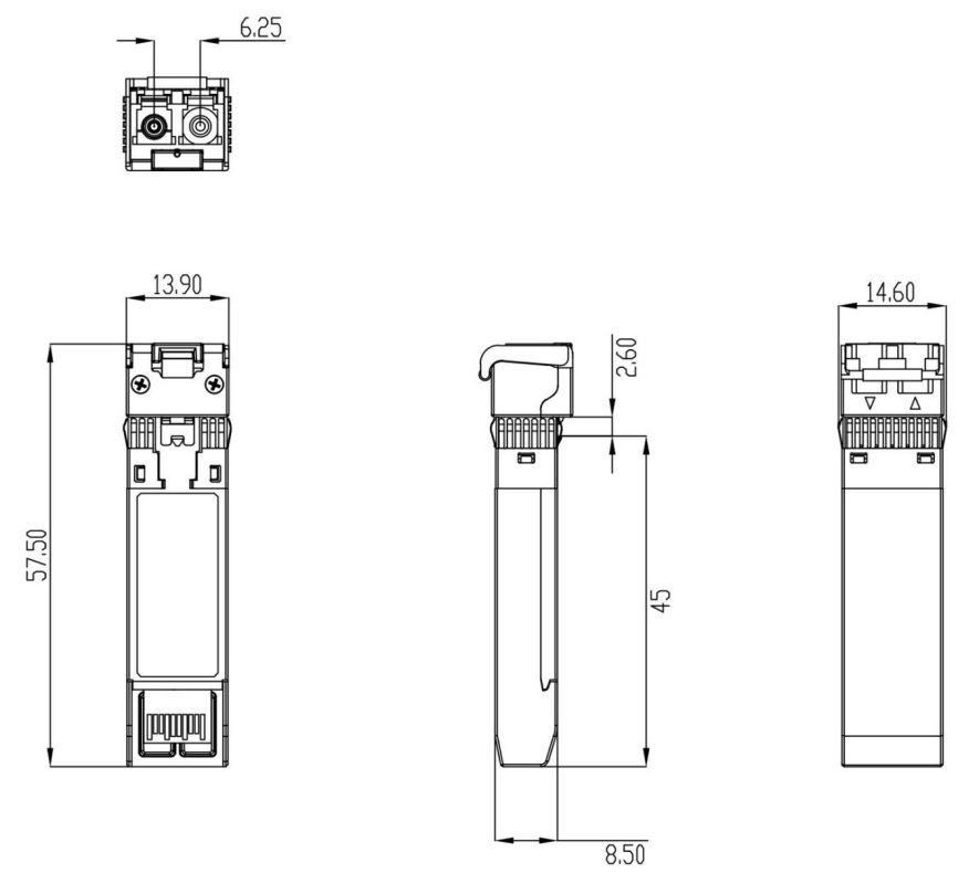 *All dimensions are ±0.2mm unless otherwise specified
ORDERING INFORMATION
Part Number |
TX |
RX |
Link |
DDM |
Mode |
Temp. |
8330-225D-V1 |
1310nm |
1260nm~1620nm |
40km |
Yes |
Single-mode |
0~70°C |
8330-225DE-V1 |
1310nm |
1260nm~1620nm |
40km |
Yes |
Single-mode |
-40~85°C |
8330-205D-V1 |
1550nm |
1260nm~1620nm |
40km |
Yes |
Single-mode |
0~70°C |
8330-205DE-V1 |
1550nm |
1260nm~1620nm |
40km |
Yes |
Single-mode |
-40~85°C |
NOTE: Distances are indicative only. To calculate a more precise link budget based on specific conditions in your application, please refer to the optical characteristics.